
Surging Demand for Laser Drilling and Plasma Dicing Equipment in Advanced Packaging
Advanced packaging has become one of the semiconductor industry’s most important growth engines, and it is now pulling a surprising set of process tools into the spotlight. Among the most in-demand are laser drilling and plasma dicing equipment. These machines sit close to the heart of heterogeneous integration, fan-out packaging, wafer thinning, TSV formation, glass substrate processing, and other advanced flows where precision, yield, and throughput matter enormously. As packaging moves from a back-end afterthought to a strategic platform, the equipment used to shape, open, and separate materials has become just as important as the dies themselves.
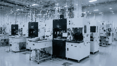
What makes this trend especially interesting is that it reflects a deeper change in semiconductor manufacturing. The push toward AI, high-performance computing, 5G, automotive electronics, and chiplet-based architectures is increasing the complexity of every package. Wafers are thinner, interconnects are denser, materials are more varied, and tolerances are tighter. Traditional mechanical approaches to drilling and dicing are increasingly being pushed to their limits. Laser and plasma tools are stepping in because they can handle delicate structures with better precision and less damage. In a sense, the rise of these tools is a sign that advanced packaging has become a precision manufacturing discipline of its own.
Why These Tools Matter Now
The reason demand is surging is straightforward: advanced packaging keeps getting more demanding. In older packaging flows, dicing a wafer or drilling a substrate was mostly about separating parts and opening pathways. In modern advanced packaging, those same steps can determine whether a fine-pitch system succeeds or fails. Laser drilling is used for via formation, micro-hole opening, substrate processing, ABF drilling, and glass-related structures. Plasma dicing is used to singulate wafers and packages with minimal mechanical stress and low kerf loss. Both processes are critical when the package is fragile, thin, or highly integrated.
The shift to heterogeneous integration amplifies this need. When a package includes multiple dies, HBM, interposers, redistribution layers, and thin substrates, the margin for error shrinks dramatically. Mechanical dicing can introduce cracks, chipping, or contamination. Conventional drilling can be too coarse or too stressful for delicate materials. Laser and plasma approaches offer a cleaner, more controlled path. That is why the market is seeing intense interest from IDMs, foundries, OSATs, and substrate makers alike.
Laser Drilling in Advanced Packaging
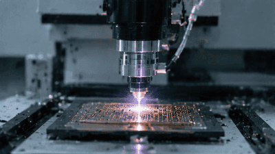
Laser drilling is one of the most versatile tools in advanced packaging. It can be used for through-silicon vias, through-glass vias, substrate openings, microvias, and other features that require precision and repeatability. Depending on the material and process, laser systems can provide high aspect ratio drilling, low thermal damage, and precise control over hole geometry. That makes them especially valuable in packages that use glass core substrates, fan-out technologies, or extremely fine routing layers.
The demand is rising because the packages themselves are changing. As routing density increases, the via structures needed to connect layers must become smaller, cleaner, and more consistent. Laser drilling provides a way to create those structures without relying on purely mechanical or chemical methods that may be less flexible for new materials. It is also attractive because it can be adapted for different substrate types, including silicon, glass, organic materials, and composite stacks.
There is another practical reason for the demand: throughput. Modern advanced packaging lines need to move fast enough to support volume production. Laser drilling systems are increasingly designed for multi-beam or high-speed operation, which makes them more suitable for industrial-scale deployment. The more advanced the packaging flow, the more likely it is to require laser equipment somewhere in the line.
Plasma Dicing and the Yield Equation
Plasma dicing solves a different but equally important problem. Traditional sawing or blade dicing can create mechanical stress, chips, and microcracks, especially in thin wafers or delicate fan-out structures. Plasma dicing uses dry etching to separate dies with minimal physical contact, which can reduce damage and improve yield. This is particularly attractive in advanced packaging, where wafers may be extremely thin or structurally fragile after back-end processing.
The growing appeal of plasma dicing is tied closely to heterogeneous integration. As packages include more layers and more sensitive structures, singulation becomes harder to do safely. Plasma dicing offers low kerf loss and better edge quality, which can translate directly into more usable dies per wafer and fewer reliability problems after assembly. In a cost-sensitive environment, that yield benefit matters a great deal.
It also helps that plasma dicing integrates well with advanced packaging flows such as fan-out wafer-level packaging, 3D stacking, and dicing-before-grinding processes. These use cases often involve ultra-thin wafers or complex layer stacks where conventional mechanical methods may introduce too much risk. Plasma tools may be more expensive upfront, but they can justify themselves by preserving die integrity and reducing scrap. That is why demand is growing not only in R&D labs but also in production lines.
Advanced Packaging Changes the Tool Market
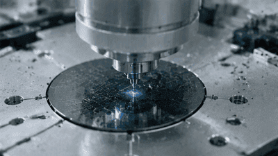
The rise of advanced packaging has effectively reshaped the equipment market. Laser drilling and plasma dicing were once specialized tools used in a limited number of applications. Now they are central enablers for many of the most valuable package types in the semiconductor industry. That means equipment suppliers are no longer selling simple process modules. They are selling strategic capacity.
This shift has several implications:
- More tool diversity. Customers need systems that can work across wafers, panels, substrates, and new materials.
- More process integration. Drilling and dicing now need to fit into tightly coordinated packaging flows.
- Higher precision requirements. As packages shrink and interconnect density rises, tolerance windows are narrowing.
- Greater yield pressure. A defect at the drilling or dicing step can affect the entire advanced package.
The result is a tool market that is growing not just because more units are needed, but because each unit has to perform more sophisticated work. This is what makes laser drilling and plasma dicing equipment so important in the current cycle.
Why AI and HPC Are Driving the Demand
AI and HPC are the biggest demand engines behind advanced packaging, and they are also driving equipment demand. High-end accelerators and switching chips depend on advanced interconnect schemes, HBM integration, and increasingly large packages. Those packages often require laser drilling for vias and plasma dicing for precise singulation, especially when the dies and substrates become thinner and more fragile.
The demand is not just for more chips. It is for more complex chips, which means more complex packaging. A single AI accelerator package may require a large logic die, multiple memory stacks, and a high-density substrate or interposer. That creates more opportunities for packaging-related defects and more need for precise process control. The better the drilling and dicing equipment, the more likely the package is to meet performance and reliability targets.
This creates a reinforcing loop. AI drives advanced packaging demand, advanced packaging drives laser and plasma equipment demand, and better equipment enables more sophisticated AI hardware. The result is a classic industrial flywheel.
Panel-Level and Glass-Based Packaging Add More Pressure
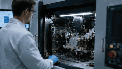
Another major reason demand is rising is the growth of panel-level packaging and glass-based substrates. These technologies are attractive because they promise better material utilization, larger process areas, and potentially lower cost at scale. But they also require tools that can handle different materials and larger formats with high precision.
Laser drilling is especially important for glass core substrates and through-glass vias. Glass is mechanically different from silicon and organic substrates, which means drilling it cleanly requires carefully tuned laser processes. Plasma dicing also becomes more valuable as large or delicate panel-based structures need to be singulated without damage. The more the industry explores these new substrate formats, the more critical these tools become.
This is a good example of how one technology trend creates demand in another part of the supply chain. The move toward larger-format advanced packaging is not only about packaging efficiency. It is also about equipment capable of processing new materials at industrial scale.
Yield, Damage, and Reliability
In advanced packaging, the cost of poor singulation or drilling is high. A small defect can affect bonding, thermal performance, electrical reliability, or long-term mechanical stability. That is why the choice of equipment matters so much. Laser drilling and plasma dicing are attractive because they reduce physical stress, which can improve yield and reliability compared with more traditional methods.
For many advanced packages, edge quality is critical. A rough cut or damaged via can become a future failure site during thermal cycling or mechanical stress. Plasma dicing reduces this risk by avoiding blade contact, while laser drilling offers better control over feature formation. The advantage is not just a prettier process. It is a more reliable package.
This reliability angle is especially important in automotive, industrial, and AI server applications, where long service life and high operating stress are part of the design brief. A package that looks good on the line but fails in the field is too expensive to tolerate. Equipment that helps avoid those failures has real strategic value.
Equipment Innovation Is Accelerating
As demand rises, equipment vendors are responding with more sophisticated platforms. Multi-beam laser systems, higher throughput plasma dicing chambers, and integrated process lines are all being developed to meet the needs of advanced packaging customers. The focus is on improving precision while preserving productivity, which is not an easy balance to strike.
Some of the key innovation themes include:
- Higher throughput without sacrificing feature quality.
- Better control over thermal impact and debris.
- Compatibility with warpage-sensitive substrates and thin wafers.
- Integration with upstream and downstream packaging steps.
The equipment race is not just about one tool model versus another. It is about building a process ecosystem that can handle the entire advanced packaging flow. Vendors that can support that ecosystem are likely to benefit the most from the surge in demand.
Who Benefits Most
Several groups stand to benefit from the growing demand for laser drilling and plasma dicing equipment. Equipment suppliers obviously gain, but so do advanced packaging houses, substrate makers, and chip designers who need more process flexibility. Foundries and OSATs that can offer these capabilities at scale are better positioned to win AI and HPC programs.
There is also a regional dimension. Countries and regions trying to build domestic advanced packaging ecosystems need access to these tools if they want to compete in high-value heterogeneous integration. That means the demand is not only commercial but strategic. Equipment capability is becoming part of semiconductor sovereignty discussions in more than one region.
From a customer perspective, the benefit is better package quality and more design freedom. If laser drilling and plasma dicing are available and mature, engineers can pursue more ambitious packaging architectures. That opens the door to more innovation upstream in chip design as well.
The Road Ahead
The most likely future is that laser drilling and plasma dicing become standard parts of advanced packaging toolkits rather than specialty exceptions. As materials diversify and package complexity rises, these tools will be needed in more process flows, not fewer. Their role will likely expand across fan-out, FOPLP, TSV, glass substrates, and next-generation 3D integration.
The next phase of growth may also be driven by two themes: larger formats and finer features. Panels are getting bigger, and vias and dicing lines are getting smaller. That combination is a demanding one. It will reward tools that can deliver both high precision and high throughput.
Over time, the line between front-end and back-end equipment may blur even further. Advanced packaging already behaves like a hybrid of both, and laser drilling plus plasma dicing are perfect examples of that crossover. They are not just support tools. They are part of the new semiconductor core.
Conclusion
The surging demand for laser drilling and plasma dicing equipment is a clear sign that advanced packaging has entered a more mature and more demanding phase. Heterogeneous integration, AI, HPC, and new substrate formats are all pushing packaging flows toward greater precision, lower damage, and better yield. That, in turn, is driving a strong need for tools that can shape and separate materials with far more control than traditional methods.
Laser drilling and plasma dicing are becoming indispensable because they solve problems that advanced packaging cannot afford to ignore. They help create cleaner vias, safer singulation, better yield, and more reliable packages. As the industry keeps moving toward more complex systems-in-package and multi-die architectures, these equipment categories will remain at the center of the advanced packaging story.
You May Like

Narrowing Spread Between NAND Spot and Contract Prices in 2026 – A Signal
By 2026, one of the most watched metrics in the NAND flash market has started to shift in a subtle but meaningful way: the spread between spot prices and long‑term contract prices is narrowing. For casual observers, this may look like just another incremental change in a notoriously volatile industry. For memory makers, module houses, device OEMs, and data center buyers, however, a tightening gap between spot and contract prices is a signal—a reflection of evolving supply–demand balance, risk perceptions, and strategic behavior on both sides of the market.

Price Divergence Trading Strategies Between NAND Flash and DRAM ETFs
NAND flash and DRAM sit at the core of AI storage and computing power. Both are memory, but they are not the same business. DRAM is main memory—fast, volatile, and central to high‑bandwidth workloads like AI training and inference. NAND is non‑volatile storage—slower than DRAM, but crucial to persistent data and large‑scale object storage. The cycles that drive their pricing and margins overlap, yet they often diverge. That divergence is where trading strategies between NAND and DRAM ETFs become interesting.

China’s HBM Localization Progress: The Catch-Up Pace of CXMT and XMC
China’s drive to localize advanced memory technologies has accelerated over the past several years. High-Bandwidth Memory (HBM) sits near the center of that strategy because it is integral to AI accelerators, high-performance computing (HPC) and other strategic compute platforms. Two domestic players—ChangXin Memory Technologies (CXMT) and XMC (Xianghui Memory, commonly referred to as XMC)—have become focal points in assessing how quickly China can close the gap with international incumbents on HBM die, stacking, and packaging.

Thermal Simulation Challenges and Solutions in 3DIC AI Chip Design
As AI workloads push chips to deliver ever higher compute density, designers are increasingly turning to three‑dimensional integration (3DIC) to stack dies vertically and pack more functionality into limited footprints. While 3DIC architectures unlock significant performance and bandwidth advantages, they also introduce complex thermal behaviors that are far harder to predict and manage than in traditional 2D layouts.

An Attempt at Compiling a Memory+Compute Fusion Thematic Index – A Dual-Track Framework
Most AI investors talk about “compute” as if it were the whole story: GPUs, accelerators, chips, cores. But every one of those cores needs somewhere to read from and write to. Memory and storage define how wide the data highway really is. In practice, AI performance is a fusion of compute and memory, not a solo act. So why do so many indices and ETFs separate them into different silos—one for semiconductors, one for memory, one for data centers—when the actual workloads keep blending them?
Surging Demand for Laser Drilling and Plasma Dicing Equipment in Advanced Packaging
Advanced packaging has become one of the semiconductor industry’s most important growth engines, and it is now pulling a surprising set of process tools into the spotlight. Among the most in-demand are laser drilling and plasma dicing equipment. These machines sit close to the heart of heterogeneous integration, fan-out packaging, wafer thinning, TSV formation, glass substrate processing, and other advanced flows where precision, yield, and throughput matter enormously. As packaging moves from a back-end afterthought to a strategic platform, the equipment used to shape, open, and separate materials has become just as important as the dies themselves.

D2D Interface Bandwidth and Latency Comparison in Chiplet Architectures
Chiplet architecture has turned the package into a real performance battleground. Once multiple dies are placed side by side or stacked within the same advanced package, the quality of the die-to-die, or D2D, interface becomes one of the most important determinants of system behavior. Bandwidth is no longer a nice-to-have metric, and latency is no longer a small implementation detail. Together, they shape whether a chiplet system feels nearly monolithic or frustratingly fragmented.

Stock Selection Logic and Alpha Validation of ESG-Themed Semi ETFs
Semiconductor themed ETFs are no longer just about growth and cycles. A growing subset now layers environmental, social, and governance (ESG) criteria on top of traditional sector exposure. These ESG semi ETFs promise two things at once: access to one of the market’s most powerful secular themes, and alignment with sustainability and governance standards. The pitch is appealing, but it raises two hard questions. First, how exactly are these stocks being selected? Second, does the ESG overlay help, hurt, or leave alpha unchanged?